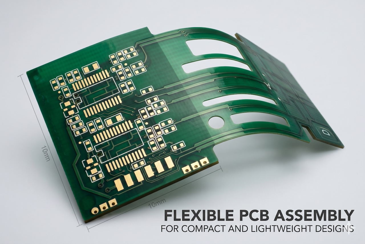
The world of electronics is transforming quickly, with consumers and industries requiring products that are smaller, more lightweight, wiser, and more robust than ever before. From mobile phones and laptops to wearable technology, automotive systems, and medical supplies, modern technologies are expected to deliver outstanding performance while occupying minimal space. To meet these requirements, manufacturers rely on advanced circuit technologies that enable more compact product designs without compromising reliability. One of the most adequate explanations on this site is Flexible PCB Assembly.
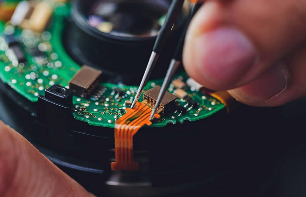
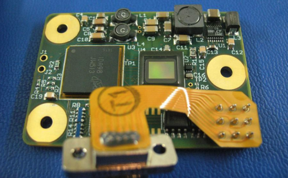
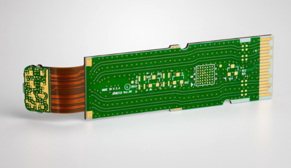
Flexible PCB Assembly guides the manufacturing and element mounting procedure brought out on bendable printed circuit boards created from flexible materials such as polyimide or polyester. The growing popularity of compact electronics has significantly increased the use of flexible PCB assemblies. Smartphones use flex circuits to connect cameras, displays, batteries, and buttons within particularly restricted internal spaces. Smartwatches and fitness bands rely on lightweight circuits that fit into small wearable form factors. In the automotive sector, flexible PCBs are utilized in detectors, dashboards, lighting systems, and infotainment management, where space-saving designs are necessary. Medical devices such as portable monitors, hearing aids, and imaging equipment also benefit from the lightweight and dedicated nature of flexible circuit assemblies. Following flexible printed circuit board design guidelines delivers dedicated performance, enhanced resilience, and efficient use of space in compact electronic products.
Expert’s Insight:
“Flexible PCB solutions combine durability, reduced weight, and space-saving benefits.”
Source: Wonderful PCB
1. What is Flexible PCB Assembly?
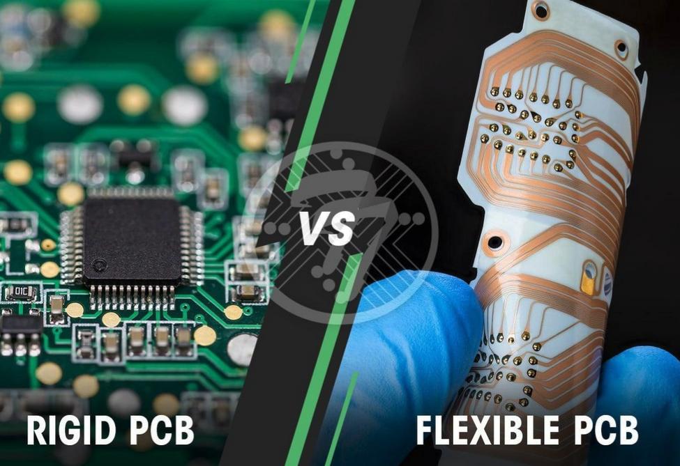
Flexible PCB assembly is the procedure of manufacturing and assembling electronic circuits on flexible insulating materials such as polyimide or polyester. Rather than rigid fiberglass boards, flexible PCBs use delicate and bendable substrates that can fit compact product shapes.
The assembly procedure affects:
- Manufacturing copper traces on a flexible substrate
- Applying solder mask and surface finish
- Testing and inspection
- Designing the flexible circuit layout
- Drilling and plating holes
- Mounting electronic components using SMT or THT
- Final integration into products
Flexible PCB assembly allows lightweight, space-saving, and admirably dedicated electronic keys.
Expert’s Insight:
“Flexible PCB technology helps eliminate bulky wiring and connectors.”
2. Importance of Flexible PCB Assembly in Modern Electronics:
As devices shrink in dimensions, internal space becomes restricted. Conventional rigid PCBs may require connectors, wires, and considerable boards. Flexible PCB assembly decodes this issue by substituting bulky wiring harnesses with delicate, bendable circuits.
Key importance includes:
- Minimizes product weight
- Enhances reliability by reducing connectors
- Improves aesthetics in slim devices
- Supports complex three-dimensional packaging
- Allows moving or dynamic applications
- Reduces overall product size
- Improves signal transmission
- Allows moving or dynamic applications
Because of these advantages, flexible PCB assembly has become necessary in developed electronics manufacturing.
3. Primary Materials Used in Flexible PCB Assembly:
Flexible PCB performance relies heavily on material selection.
3.1. Base Substrate
The most typical substrate is polyimide because it presents:
- Excellent flexibility
- Chemical resistance
- High heat resistance
- Strong mechanical strength
Polyester is another choice for low-cost applications.
3.2. Copper Foil
Copper foil forms conductive paths. Rolled annealed copper is selected because it withstands repeated bending more sufficiently than electro-deposited copper.
3.3. Adhesives
Adhesives bond copper foil to substrate layers. Adhesiveless laminates are also utilized for more suitable thermal performance.
3.4. Coverlay
Coverlay covers copper traces and performs like a solder mask on rigid boards.
3.5. Stiffeners
FR4 or polyimide stiffeners are counted where connectors or features need additional support.
4. Table of Common Flexible PCB Materials and Uses:
| Material | Function | Advantages | Common uses |
|---|---|---|---|
| Polyester | Base substrate | Low cost, lightweight | Consumer electronics |
| Coverlay | Protection layer | Flexible insulation | Flex boards |
| Polyamide | Base substrate | Heat-resistant, flexible | Medical, aerospace |
| FR4 Stiffener | Reinforcement | Mechanical support | Connector zones |
| Copper Foil | Protection layer | High conductivity | All circuits |
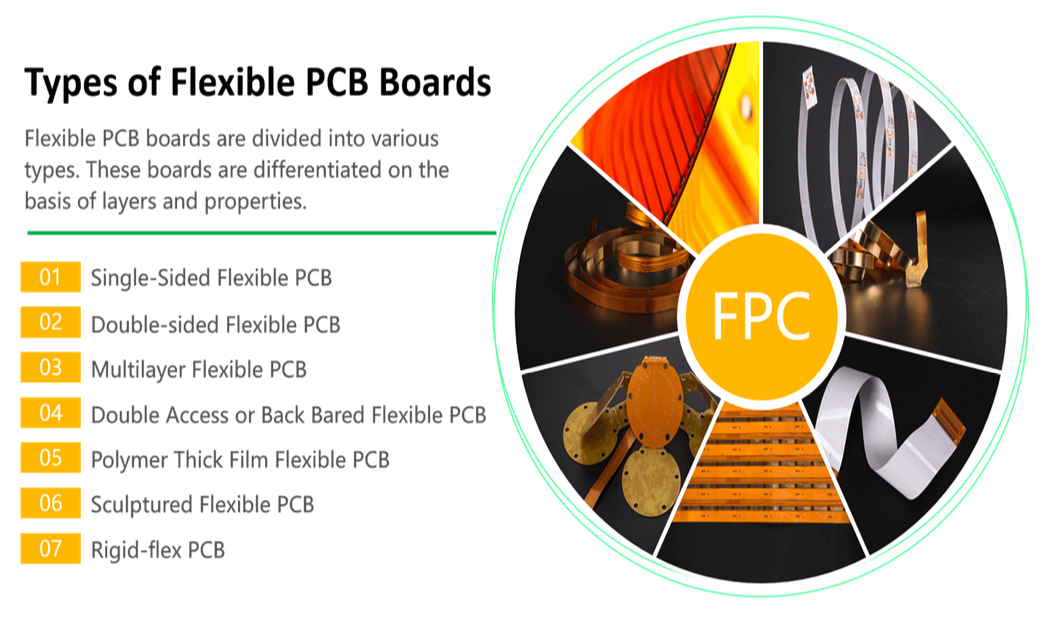
5. Classes of Flexible PCBs:
5.1 Single-Sided Flex PCB:
Possesses one conductive copper layer. Operated in uncomplicated, low-cost products.
5.2 Double-Sided Flex PCB:
Has copper layers on each side. Fit for more intricate circuits.
5.3 Multilayer Flex PCB:
Utilizes numerous conductive layers for modern electronics.
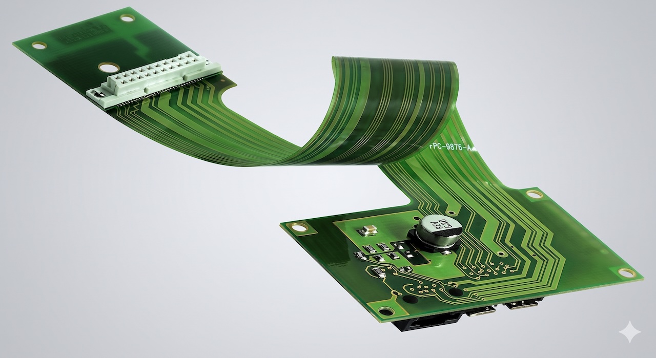
5.4 Rigid-Flex PCB:
Converges rigid and flexible board sections. Famous in aerospace and medical devices.
5.5 Sculptured Flex PCB:
Operates variable copper thickness for power and signal sections.
6. Benefits of Flexible Printed Circuit Board Assembly for Compact and Lightweight Designs:
6.1. Decreased Weight
Flexible circuits are much more delicate than rigid boards and the harnesses of the wire. This is crucial for transportable electronics and aerospace systems.
6.2. Space Saving
They can turn, fold, or bind around elements, permitting effective usage of internal product space.
6.3. High Dependability
More infrequent connectors and wires decrease failure pinpoints.
6.4. Better Airflow
Compact configurations enhance cooling and airflow inside products.
6.5. Faster Assembly
Combined flexible circuits facilitate product assembly.
6.6. Improved Shock Resistance
Flexible boards absorb vibration more usefully than rigid boards.
6.7. Dynamic Flexing Capability
Some methods permit repeated movement, model for hinges and moving machines.
7. Flexible PCB Assembly Process:
Step 1: Circuit Design and Engineering
Engineers make the circuit schematic and PCB design utilizing CAD software. Essential factors possess:
- Trace width
- Component placement
- Bend radius
- Thermal needs
- Layer count
Step 2: Material Preference
Manufacturers choose substrate thickness, copper kind, adhesive method, and surface finish based on product requirements. For lightweight products, ultra-thin materials are selected.
Step 3: Imaging and Etching
Copper-clad flexible laminate is coated with photoresist. UV imaging transfers the circuit pattern. Chemical etching removes unwanted copper, leaving traces.
Step 4: Drilling and Via Formation
Laser or mechanical drilling makes holes for interconnections. Vias are plated with copper.
Step 5: Coverlay Lamination
Protective coverlay film is laminated over traces, while ditching pads are disclosed for soldering.
Step 6: Surface Finish Application
Pads receive defensive finishes such as:
- OSP
- Tin
- ENIG
- Immersion silver
These finishes enhance solderability.
Step 7: Component Placement
Using automated pick-and-place machines, components are accurately placed. Standard features include:
- Resistors
- Connectors
- ICs
- Capacitors
- LEDs
Step 8: Soldering Process
Reflow soldering is generally utilized for SMT components. Temperature management is crucial because flexible materials respond differently from rigid boards.
Step 9: Inspection and Testing
Boards undergo:
- X-ray inspection
- Functional testing
- Flex cycle testing
- AOI inspection
- Continuity testing
Step 10: Final Assembly Integration
Constructed flexible PCB assemblies are incorporated into end products.
8. Table of Flexible PCB Assembly Steps and Purpose:
| Step | Process | Purpose |
|---|---|---|
| Material selection | Match performance needs | |
| Placement | Mount components | |
| Drilling | Create vias and holes. | |
| Surface finish | Improve soldering | |
| Soldering | Electrical connection | |
| Final integration | Install into the device. | |
| Design | Create a functional layout. | |
| Etching | From copper traces | |
| Coverlay | Protect circuity | |
| Testing | Ensure quality |
9. Design Rules for Flexible PCB Assembly:
Appropriate design is essential for long life and arrangement.
9.1. Bend Radius
Sharp bends may crack copper traces. Suggested bend radius relies on consistency.
9.2. Trace Routing
Utilize curved traces rather than sharp corners.
9.3. Component Placement
Avoid placing elements in bend areas.
9.4. Stiffener Use
Utilize stiffeners under connectors or serious roles.
9.5. Copper Balancing
Balanced copper controls warping.
9.6. Layer Alignment
Keep precise registration in multilayer boards.
10. Applications of Flexible PCB Assembly:
10.1. Consumer Electronics
Operated in smartphones, tablets, cameras, earbuds, and laptops.
10.2. Medical Devices
Discovered in hearing aids, diagnostic instruments, wearable monitors, and imaging systems.
10.3. Automotive Industry
Utilized in dashboards, detectors, airbags, lighting techniques, and infotainment.
10.4. Aerospace and Defence
Perfect for satellites, avionics, drones, and communication procedures.
10.5. Industrial Tools
Operated in robotics, automation systems, detectors, and compact regulators.
10.6. Wearable Technology
Smartwatches and wellness devices depend heavily on flex circuits.
11. Why is Flexible PCB Assembly Best for Lightweight Products?
Numerous industries concentrate on decreasing product weight to enhance portability and energy efficiency.
11.1. Smartphones
Small procedure needs folded internal circuits.
11.2. Drones
Reduced weight enhances flight time.
11.3. Medical Devices
Transportable healthcare tools benefit significantly.
12. Challenges in Flexible PCB Assembly
Although highly valuable, flexible PCB assembly has some challenges.
12.1. Higher Initial Cost
Materials and manufacturing procedures can be more costly than fixed PCBs.
12.2. Complex Design Requirements
Needs experienced engineering.
12.3. Delicate Handling
Thin materials require attentive processing.
12.4. Thermal Management
Compact configurations may trap heat.
12.5. Specialized Equipment
Manufacturers require progressive assembly appliances.
13. Quality Control in Flexible PCB Assembly:
Dedicated products rely on rigid quality measures.
13.1. Visual Inspection
Assessments include scratches, alignment, and imperfections.
13.2. AOI Systems
Notice soldering mistakes automatically.
13.3. Electrical Testing
Affirms circuit continuity.
13.4. Dynamic Bend Testing
Tests duplicated flexing durability.
13.5. Environmental Testing
Reviews heat, humidity, and trembling resistance.
14. Future Directions in Flexible PCB Assembly:
Technology persists, evolving fast.
14.1. Ultra-Thin Electronics
Actual thinner circuits for foldable machines.
14.2. Flexible Shows Integration
Circuits merged with screens.
14.3. Printed Electronics
Low-cost printed conductive circuits.
14.4. IoT Devices
Compact detectors and connected devices.
14.5. Medical Wearables
Rising request for body-friendly electronics.
14.6. Sustainable Materials
Environment -friendly substrates and recyclable methods.
15. How to Select a Flexible PCB Assembly Manufacturer:
Choose a supplier with:
- Flex PCB experience
- Quality certifications
- Fast prototyping
- Reliable delivery
- Strong engineering support
- Modern SMT lines
- Testing capability
- Competitive pricing
16. Best Techniques for Prosperous Flexible PCB Projects:
Choose the correct materials, use lightweight components, verify thermal behavior, use trusted assembly partners, plan bend zones early, avoid overloading flex areas, perform prototype testing, and optimize for manufacturability.
Conclusion
Flexible PCB Assembly for compact and lightweight designs has changed current electronics manufacturing. By replacing rigid, heavy boards and wiring systems, flexible PCBs enable slimmer, lighter, and more effective solutions across numerous enterprises. Their ability to bend, fold, and fit into familiar areas makes them perfect for smartphones, medical devices, wearables, automotive systems, aerospace tools, and industrial management. The assembly process applies detailed structure, material selection, precision manufacturing, constituent support, and strict quality control. Although initial prices and configuration complexity may be higher, the long-term advantages include enhanced dependability, reduced weight, space savings, and improved product arrangement.
Share this post
Author

Read the latest articles from Shahid Latif
How to Restyle Short Video Clips with Video-to-Video AI

June 5, 2026
You come back from a shoot with footage that’s good enough to use. The lighting works, the movement feels natural, and a few clips could easily become social media teasers. Then you hit the usual wall: making them look anime-inspired, illustrated, or cinematic often means learning effect-heavy editing, testing [...]
Learn moreAI Video Enhancer: Your Videos Don’t Look Professional? Here’s the Fastest Fix

June 1, 2026
Ever invest hours into making a video only to upload and find it looks blurry, dull, or just… not professional?
Learn moreLeave a comment
All comments are moderated. Spammy and bot submitted comments are deleted. Please submit the comments that are helpful to others, and we'll approve your comments. A comment that includes outbound link will only be approved if the content is relevant to the topic, and has some value to our readers.
Comments (0)
No comment