In semiconductor manufacturing, success is measured in microns. The slightest variation will affect performance, reliability, and ultimately output. With new geometries being scaled down, along with increasingly complex architectures, precision equipment in the manufacturing process has become necessary.
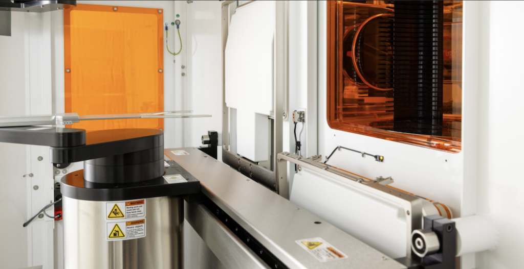
The changeover has as its focal point the Equipment Front End Module (EFEM) module. This module has become crucial in the handling of the wafers and in the integration of the tools effectively. It has become crucial for fabs as it ensures the safe transfer of the wafers from one chamber to the other with no defects.
Following the growing demand for sophisticated logic chips, memory solutions, and AI processors, companies are being challenged to increase their production without affecting the quality of their product. This is where precision technologies are changing the dynamics of yield realization at a mass production level.
Why Precision Is the Backbone of Modern Fabs
Today's semiconductor environment is much more complex than traditional manufacturing. Several processing steps, structures at the nanometer level, and strict cleanliness standards demand absolute control at every stage. The semiconductor fabrication tools today are no longer stand-alone machines, but integrated ecosystems for accuracy and repeatability with real-time monitoring.
The EFEM is an interface between wafers and processing equipment. Reducing contaminant exposure by keeping controlled environments and properly aligning wafers, EFEM systems provide process stability. In this integration, EFEM supports tighter control in semiconductor processes, which is so crucial for maintaining uniformity among thousands of wafers.
From lithography and etching to deposition and cleaning, each process relies on precision engineering in semiconductors. Advanced automation and robotics today ensure consistency in the handling of wafers, minimizing human touches, and reducing variability that can impact yields.
The Growing Importance of Yield Optimization
The profit margins of chip production are directly affected by yield. Where a minute change in the percentage of yield translated to millions of additional revenues every year in the past, the current focus of the semiconductor industry has shifted to optimizing yields rather than emphasizing other key performance factors.
Precision tools make the following capabilities possible in fabs:
- Identify defects earlier in the process
- Maintain tighter dimensional tolerances
- Improve wafer-to-wafer and lot-to-lot consistency
- Eliminate rework and scrap
With shrinking nodes and the advent of advanced packaging technology, yield enhancement cannot be furthered without high-accuracy and high-sensitivity equipment.
Key Precision Tools Transforming Semiconductor Fabrication
1. Wafer Fabrication Precision Tools
Wafer fabrication precision ordains the accurate pattern of transfer, layer thickness control, and alignment across multiple process steps. These machines are designed to operate within very narrow tolerances, typically measured in nanometers.
Their benefits include:
- Improved pattern fidelity
- Reduced overlay errors
- Stable processing in high-volume production
Such precision becomes even more critical as fabs move toward advanced nodes and heterogeneous integration.
2. Semiconductor Metrology and Inspection Tools
Metrology and inspection systems represent the data backbone of fabrication, as they measure critical dimensions and film thickness, and detect surface defects in real time. Without them, maintaining yield consistency would be nearly impossible.
The semiconductor metrology and inspection tools help the manufacturers:
- Identify deviations before they escalate
- Allow for fast corrective actions
- Support data-informed decision-making
Precise data is fed into the control systems, which enhances a fab's visibility into process health and performance trends.
3. Advanced Semiconductor Manufacturing Equipment
These modern fabs depend upon semiconductor manufacturing equipment incorporating automation, robotics, sensors, and AI-driven analytics. These systems are designed not only to produce but also to continually optimize.
Key advantages include:
- Higher throughputs with consistent quality
- Reduced downtown by way of predictive maintenance
- Improved tool-to-tool matching
These tools, combined with EFEM systems and automated material handling, further enhance fab efficiency.
How Precision Tools Improve Semiconductor Process Control
Effective semiconductor process control depends on maintaining uniformity across thousands of operations performed daily. Precision tools allow manufacturers to establish stable baselines and rapidly respond to variations.
Below is a simplified view of how different tools contribute to process control and yield improvement:
| Precision Tool Type | Primary Function | Impact on Yield |
|---|---|---|
| EFEM Systems | Wafer handling and contamination control | Reduces handling defects |
| Metrology Tools | Measurement and monitoring | Early defect detection |
| Inspection Systems | Surface and pattern analysis | Prevents defect propagation |
| Precision Robotics | Accurate wafer movement | Improves repeatability |
| Process Control Software | Data analysis and feedback | Stabilizes production |
This combination of hardware and intelligence creates a closed-loop environment where yield improvement becomes continuous rather than reactive.
Business Benefits of Precision-Driven Fabrication
The inclusion of precision tools for semiconductor manufacturing involves not only technology, but it is a strategic move as well. The fabs that place great value on precision have a competitive advantage.
Measurable Benefits Include:
- Greater Yields: Fewer defects & greater uniformity
- Operating Cost Reduction: The cost of scrap/rework
- Enhanced Throughput: More efficient processing at consistent performance
- Better product reliability: Enhanced end-device performance
Precision engineering will also promote smoother technology transitions, allowing the electronics sector to embrace newer nodes and packaging solutions easily.
With emerging markets for Artificial Intelligence, car electronics, and HPC computing, being able to ensure quality at scale is what determines success.
The Role of Automation and Robotics
It has become inseparable from precision, where advanced robotics ensure wafers are transferred smoothly, aligned accurately, and kept clean without contamination. These systems work with repeatability levels that cannot be achieved with manual handling.
Robotics creates a unified front-end environment when combined with EFEM platforms, enhancing safety, cleanliness, and efficiency. These combinations reduce variability and allow for long-term yield stability.
In the modern fab, automation is no longer optional; it forms the basis of sustainable manufacturing excellence.
Preparing for the Future of Semiconductor Manufacturing
With increasingly complex designs for semiconductor devices, fabs have to advance as well. Upgrading legacy systems and enhancing metrology and automation capabilities are key to moving forward with manufacturing that is ready for tomorrow.
It is a good time for manufacturers to analyze their fabrication environment and determine where improvement is possible. The use of advanced precision tools helps achieve greater control and competitiveness in a challenging market.
Conclusion: Precision as the Path to Sustainable Yield
For future semiconductor manufacturing, accuracy, reliability, and intelligent automation are required. Right from the fabrication tools for semiconductors to the tools used for semiconductor metrology, each has its relevance in obtaining the best possible outcome.
Precision engineering in the semiconductor industry is no longer a supporting activity; instead, it has emerged as the bedrock upon which the entire fab is based. By embracing the adoption of advanced equipment in the semiconductor industry, companies will be able to address the demands of today as well as be ready for the technologies of tomorrow.
Featured Image generated by Google Gemini.
Share this post
Leave a comment
All comments are moderated. Spammy and bot submitted comments are deleted. Please submit the comments that are helpful to others, and we'll approve your comments. A comment that includes outbound link will only be approved if the content is relevant to the topic, and has some value to our readers.
Comments (0)
No comment